Learn EasyEDA – Free ,Online PCB Design Software ( With PCB Project – Microcontroller Based System ) & VHDL Programming
What you’ll learn
Designing Single Layer , Double Layer & MultiLayer PCBs using EasyEDA PCB Tool & considering General Guidelines for Layout / PCB Design & with DRCs. Designing Surface Mount PCBs ( Single Layer & Double Layer ) Creating Library parts like Custom Components ,Schematic Modules & PCB Modules . Designing Big PCB Project for Microcontroller Based system Design . Generating Artwork Files & Creating small in-house PCB Fabrication setup . Generating Gerber File & Ordering PCBs and also BOM for Ordering Components
Requirements
Basic Understanding of Electronic Components . Basic Knowledge of Computer & Internet . Electronic Circuit concepts is advantageous . Some Patience !
Description
Hello Dear Student ,
I welcome you , for Enrolling this Course .
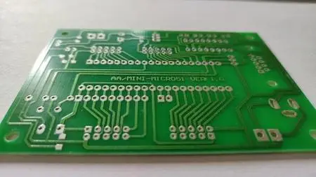
This is basically a Beginners Course with Basic Level Content focused on PCB Design using EasyEDA , a Free & On-Line PCB Design Software and it covers Content with 1-Layer , 2-Layer Through Hole type & SMT type PCB Design & also Multi-layer ( 4-Layer ) PCB Design , as a beginner’s reference suitable for Electronics Polytechnic , Engineering & University Students & Hobbyists .
Apart from PCB Design content , Added introductory level content ( At Very Basic Level ) of VHDL Programming using Xilinx ISE Webpack Software a Free Downloadable Software . You may treat the VHDL Basic Level Programming Content as a complementary Content , if you are Electronics Students .
If you are interested in Only PCB Design Content , you may skip / ignore VHDL Basic Level Programming Content .
All the Content of this Course are based on Free Softwares & either OnLine Or downloadable Softwares for Design / Programming .
1. PCB Design ( 1 Layer , 2 Layer & Multilayer 4 Layer PCB Design Examples ) using a OnLine & Free PCB Design Software “EasyEDA” ,
2. VHDL Programming using Xilinx ISE Webpack , a Free Downloadable Software ( After Registering Your Account with Xilinx Website ) .
At the beginning , the Course Title was “ Step by Step PCB Design for Electronics Projects ” , a Course in PCB Design for Beginner Level .
My approach is to continuously add & update the Content of this Course , so-that it may be helpful specifically to Electronics Polytechnic , Engineering , University Students & also to Hobbyists .
Course Update 1st : ( Feb. 2021 ) : Added Content : VHDL Programming Examples using Xilinx ISE Webpack software .
Course Published ( In Aug. 2020 ) : Content of PCB Design using EasyEDA OnLine PCB Design Software .
Description : This PCB Design Course are developed using a very Popular EasyEDA PCB Design Software , which is a Free , Web based ( OnLine ) Tool & it has huge Components & Part Library. EasyEDA PCB Tool supports to Windows platform , Linux O.S. & also runs on Mac & Android platforms,as long as there is one browser on the O.S. & connecting to Internet.
Video Contents for every stages for Professional PCB Designs are explained with separate & Short Video sessions in a simple way for better understanding,even for the Beginners .
– Schematic Design Stage
– PCB Layout Design Guidelines ( Component Placement Guidelines )
– PCB Layout Design ( Component Placement Stage )
– PCB Design Guidelines ( Track Routing Guidelines , DRCs )
– PCB Design ( Track Routing Stage )
After observing Video sessions & also for the practice purpose , I have added the PDF / Text Documents , called as – “Quick Reference Guide” , which explains the Step by Step Designing Procedure for Single Layer , Double Layer & MultiLayer PCBs for some Examples . Separate Quick Reference Guide is provided to each type of PCBs .
Some Quiz / MCQs – Multiple Choice Questions are also incorporated by adding the separate Document for its Answer Key .
In this course you will learn about –
– Creating Single Layer PCB Design – Two Examples
– Creating Single Layer Surface Mount ( SMT / SMD ) PCB Design – Example .
– Creating Single Layer PCB Design with AutoRouter – Example
– Creating Double Layer PCB Design – Two Examples
– Creating Double Layer Surface Mount ( SMT / SMD ) PCB Design – Example
– Creating Double Layer PCB Design Example with AutoRouter – Example
– Creating Multi-Layer PCB Design – Example
– Creating Schematic Module – Example
– Creating PCB Module – Example
– Creating Schematic Symbol – Example
– Creating Footprint – Example
– Creating Custom Component – Example
– Creating Big PCB Project – Microcontroller ( 8051 ) based System Design
( which is a Multisheet Design having Schematic Modules
> 8051 Micro-controller with Clock & Reset Circuit
> DC Power Supply
> ADC 0804 Circuit
> 16 x 2 Char. LCD Display )
For Entrepreneurs / who want to start the Business , I have explained the generation of Artwork Files & small Setup for PCB fabrication ( For Single Layer PCB ) .
For Electronics Professionals / Designers , I have explained the Sizable PCB Project of Micro-contoller based System Design . Also PCB Layout Guidelines / PCB Design Guidelines ( Component Placement & Track Routing Guidelines ), DRCs , Crosstalk Issues , Maximizing Grounding , MultiLayer Stackup Planning , Multisheet design etc. will be useful information .
VHDL Programming Content are explained with some Basic VHDL Programming Examples based on Combinational & Sequential Digital Logic and with Step by Step approach i.e. VHDL Program Code , Synthesis , VHDL Test Bench & Behavioral Simulation .
–––––––––––––––––––––––––––––––––––––––––––––––––––––––––––––––––––––––––––––––––-
Instructor has more than a 22 Years of Design Experience after M.Tech. in Electronics Design & Technology , which includes the Experience in Electronic Circuit Design , Embedded System / VLSI- FPGA & CPLD Design . He has experience on a variety of EDA tools & Programming Softwares / Platforms like Python3.8 ( IDLE ) , Thonny , Google Colab , Anaconda Navigator – Jupyter Notebook , Spyder Python , Xilinx ISE Tool & Xilinx Vivado Tool for Xilinx FPGAs SPARTAN6 / Artix -7 & CPLDs XC9572 / 108 with VHDL & Verilog Programming , Cypress PSOC Designer for PSOC1 & PSOC Creator for PSOC 3 & PSOC 4 , STM32CubeIDE for STM32 – ARM 32 Bit Core Based Microcontroller , Keil uVision4 for MCS-51 Family Microcontrollers , Atmel AVR Studio for ATMega32 /128 Microcontrollers , Microchip MPLAB for PIC 16 / PIC 18 Microcontrollers , Crouzet Millenium3 for PLCs Ladder programming , FBD , Arduino CC s/w for Arduino Uno Boards , Energia for MSP430 from Texas Instruments and also which includes PCB Softwares such as EasyEDA , Eagle ( Fusion 360 ) , KiCad 5.1 , Fritzing & Express PCB etc .
–––––––––––––––––––––––––––––––––––––––––––––––––––––––––––––––––––––––––––––––––-
Who this course is for:
Initially Contents were for Basic Level & then Updated the Contents for – All Levels – Beginners , Hobbyists , Teachers who are interested to Learn to Create Professional PCB Designs , by applying knowledge of Electronics . University Students , Students from Engineering colleges & Polytechnic Institutes , who want to Design the PCB for their Electronics based Academic Project . Anyone who wants to make career in PCB design . Entrepreneurs / who want to start Business in PCB Design & Fabrication setup with Low cost for Single Layer PCBs. Electronic Designers / Embedded Engineers / Electronic Circuit Design Professionals , who are new to PCB Design field .
Contents are Extended for Intermediate & Advanced Level , by adding MultiLayer PCB Design
DOWNLOAD LINK